


All Products
-
Optical Quartz Glass
-
Machining Quartz Glass
-
Quartz Glass Tube
-
Quartz Capillary Tube
-
Borosilicate Glass Tube
-
Quartz Glass Rod
-
Laser Spare Parts
-
Silicon Dioxide Sputtering Target
-
Quartz Apparatus
-
Quartz Glass Plate
-
Custom Glass Parts
-
Custom Ceramic Parts
-
Optical Manufacturing Equipment
-
Mobile Glass Cover Making Machine
-
Optical Measuring Instrument
-
Optical Crystal
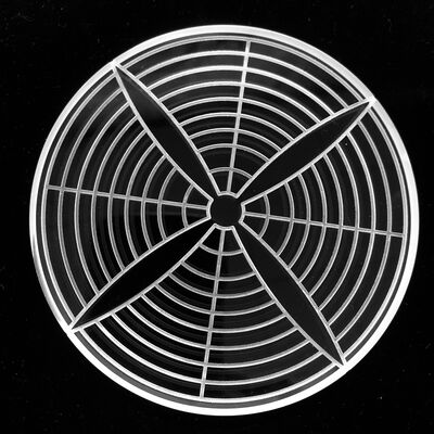
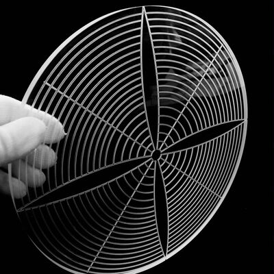
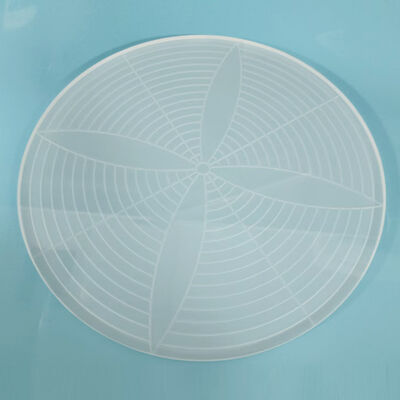
D265 Borosilicate Optical Glass Carrier Platform Low Autofluorescence High Flatness Chemical Resistant


Product Details
| Highlight | Borosilicate Optical Glass Carrier Platform,Low Autofluorescence Quartz Glass Plate,High Flatness Quartz Glass Plate |
||
|---|---|---|---|
Product Description
1. Basic Product Information
Product Name: D265 Low Autofluorescence High Flatness Borosilicate Glass Carrier Platform Base Material: Grade 1 high hydrolytic resistance D265 borosilicate optical glass Processing Technology: Double-sided optical polishing, precision grinding chamfering, ultra-clean cleaning Standard Optional Sizes: Custom square or round shapes; standard thickness 0.17–1.2mm, flatness ≤2μm, TTV total thickness variation ≤1μm
2. Main Applications
Precision monolithic machined from special low-alkali D265 borosilicate glass, this carrier features ultra-low autofluorescence, high light transmittance, acid & alkali resistance, low thermal expansion and superior flatness. It is widely used as a carrier substrate for microscopic observation, semiconductor temporary bonding, biological testing, optical lithography and precision laboratory equipment.
3. Core Advantages (vs Ordinary Borosilicate/Float Glass Carriers)
Ultra-low autofluorescence: Low-alkali D265 formula minimizes background fluorescence, eliminating stray light interference for fluorescence microscopy; Superior chemical stability: Top-grade hydrolytic resistance withstands long-term erosion of organic solvents, weak acids and alkalis with zero ion precipitation; Low thermal expansion & thermal stability: CTE matched with silicon wafers, resistant to warpage and cracking under temperature cycling and high-temperature processes; Excellent optical transmittance: High UV & visible light transmission with zero chromatic aberration, compatible with optical observation, laser and UV debonding processes; Ultra-precise flatness: Double-sided high-precision polishing with tightly controlled flatness and thickness tolerance, meeting micron-level precision requirements for semiconductors and precision optics; Low alkali & contamination-free: Low alkali content prevents cell damage and contamination of wafers/high-purity reagents, perfect for high-cleanliness manufacturing processes.
Recommended Products
